PCB Capacities and Technical Specification

Order Quantity

1-500,000

Layer

1, 2, 4, 6, up to 24 layer

Materia

FR-4, High Tg, Isola, Aluminum, Rogers, etc

PCB type

Rigid, flexible, rigid-flexible

Shape 

Rectangular, round, slots, cutouts, complex, irregular

Max PCB dimensions

1200mm*600mm

Thickness

0.2~4.0mm, Flex 0.01~0.25''

Thickness tolerance

± 10%

Copper thickness

0.5-6 oz

Copper thickness tolerance

± 0.25oz

Surface finish

HASL, LF HASL, Imm Gold, Imm Silver, OSP etc

Solder mask 

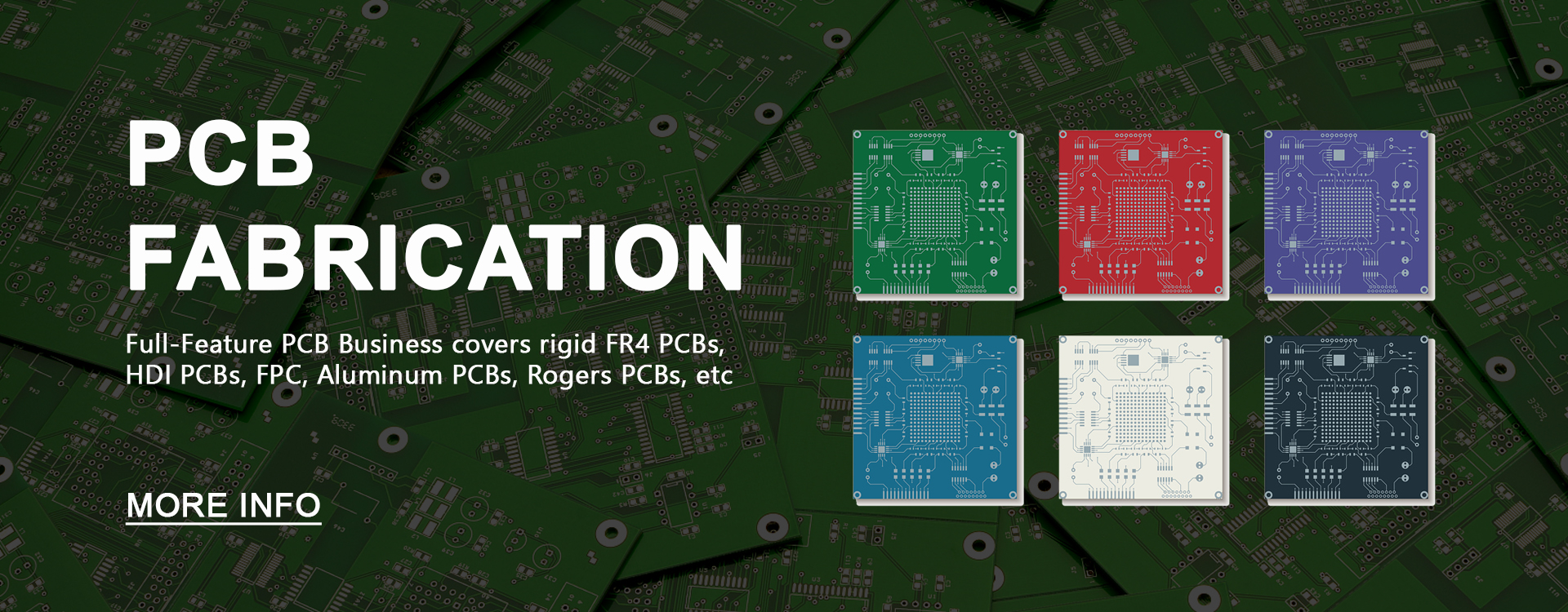
Green, red, white, yellow, blue, black, orange, purple

Silk screen

White, black

Silk screen min line width

0.006'' or 0.15mm

Min drill hole diameter

0.01'', 0.1mm or 10 mil

Min trace/gap

0.075mm or 3mil

PCB cutting

Shear, V-score, tab-routed


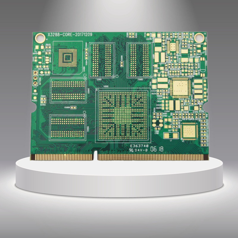
  • Rigid PCB

    A rigid PCB (Printed Circuit Board) is a traditional type of circuit board with a solid, non - bendable substrate. It is typically made of materials like fiberglass - reinforced epoxy resin. The copper layers are laminated onto this substrate, and the traces and pads are etched to create the desired electrical connections. Rigid PCBs are widely used in applications where stability and mechanical strength are required, such as in computers, servers, and industrial control systems. They can support heavy components and are suitable for complex circuit designs with high - density components.

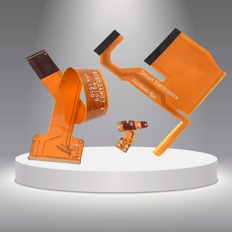
  • Flexible PCB (FPC)

    Flexible PCB, also known as FPC, is designed with a flexible substrate material, often a thin polyimide film. This allows the PCB to be bent, folded, or twisted, enabling it to fit into compact and curved spaces. The copper conductors are patterned on the flexible substrate, and vias are used for inter - layer connections. FPCs are commonly used in applications like mobile phones, wearables, and medical devices, where space constraints and the need for flexibility are crucial. They can reduce the size and weight of the overall product and improve the reliability of connections in dynamic environments.

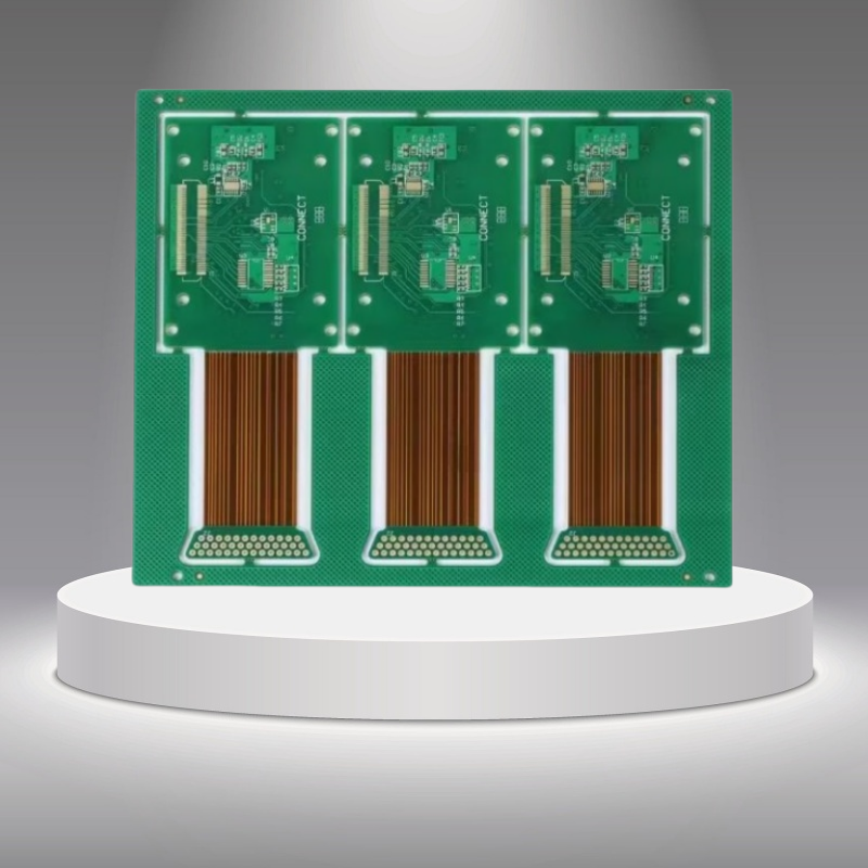
  • Rigid - Flexible PCB

    Rigid - flexible PCB combines the advantages of both rigid and flexible PCBs. It consists of rigid sections and flexible sections within a single board. The rigid parts provide mechanical support and are suitable for mounting components, while the flexible parts allow for bending and folding to connect different parts of a device. This type of PCB is often used in complex electronic systems that require both stability and flexibility, such as in aerospace and automotive applications. It simplifies the overall structure of the device by integrating multiple functions onto one board and reduces the number of connectors between different circuit boards.

  • Aluminum PCB

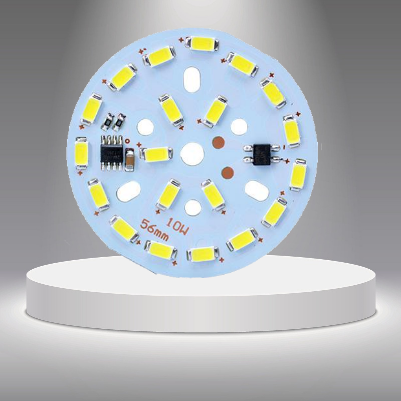
    An aluminum PCB has an aluminum substrate instead of the traditional fiberglass or other materials. The aluminum core provides excellent heat dissipation properties. A thin layer of dielectric material is coated on the aluminum, and then the copper circuit layer is laminated on top. Aluminum PCBs are widely used in high - power applications, such as LED lighting systems, power amplifiers, and power converters. The good heat - conducting ability of the aluminum substrate helps to keep the components at a suitable operating temperature, improving the reliability and lifespan of the circuit.

  • PCB Reverse Engineering Service

    PCB reverse engineering service is a specialized technical service. It involves analyzing an existing PCB to obtain its schematic diagram, component list, and design details. Advanced techniques such as X - ray inspection, scanning electron microscopy, and circuit tracing are used. This service is valuable in various situations. For example, when the original design documentation is lost, or when a company wants to improve or clone an existing product. It helps in understanding the functionality of a legacy PCB, enabling repair, modification, or reproduction of the circuit board for different purposes like product improvement, obsolescence management, or competitive analysis.

    PCBA Capabilities

    Turnkey PCBA

    PCB+components sourcing+assembly+package

    Assembly details

    SMT and Thru-hole, ISO SMT and DIP lines

    Lead Time

    Prototype : 15 work days.  Mass order : 20~25 work days

    Testing on products

    Testing jig/mold , X-ray Inspection, AOI Test, Functional test

    Quantity

    Min quantity : 1pcs. Prototype, small order, mass order, all OK

    Files needed

    PCB : Gerber files(CAM, PCB, PCBDOC)

    Components : Bill of Materials(BOM list)

    Assembly : Pick-N-Place file

    PCB Panel Size

    Min size : 0.25*0.25 inches(6*6mm)

    Max size : 1200*600mm

    Components details

    Passive Down to 0201 size

    BGA and VFBGA

    Leadless Chip Carriers/CSP

    Double-sided SMT Assembly

    Fine Pitch to 0.8mils

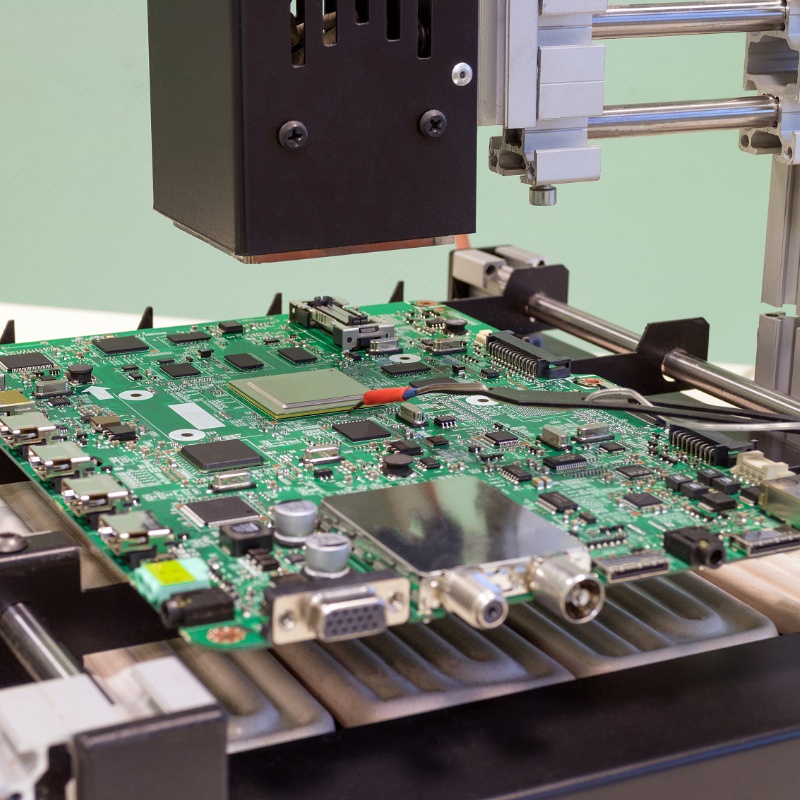
    BGA Repair and Reball

    Part Removal and Replacement

    Component package

    Cut Tape, Tube, Reels, Loose Parts

    PCB+ assembly process

          Drilling---Exposure---Plating--- Etaching & Stripping---Punching---Electrical Testing---SMT---Wave Soldering---Assembling---ICT--- Function Testing---Temperature &Humidity Testing


    • Prototype PCB Assembly

      Prototype PCB Assembly is the process of quickly and cost - effectively assembling a small number of printed circuit boards for the purpose of testing and validating a new circuit design. It allows designers to check the functionality and performance of the circuit before mass production, using techniques such as manual component placement and soldering for initial prototypes or more automated processes for more refined versions.

    • Turnkey PCB Assembly

      Turnkey PCB Assembly is a comprehensive service where a contract manufacturer takes care of the entire PCB assembly process from sourcing components, to PCB fabrication, assembly (including both SMT and DIP processes), testing, and finally delivering the fully assembled and tested PCBs to the customer. It provides a one - stop solution for customers who want to outsource the entire production process.

    • SMT / DIP

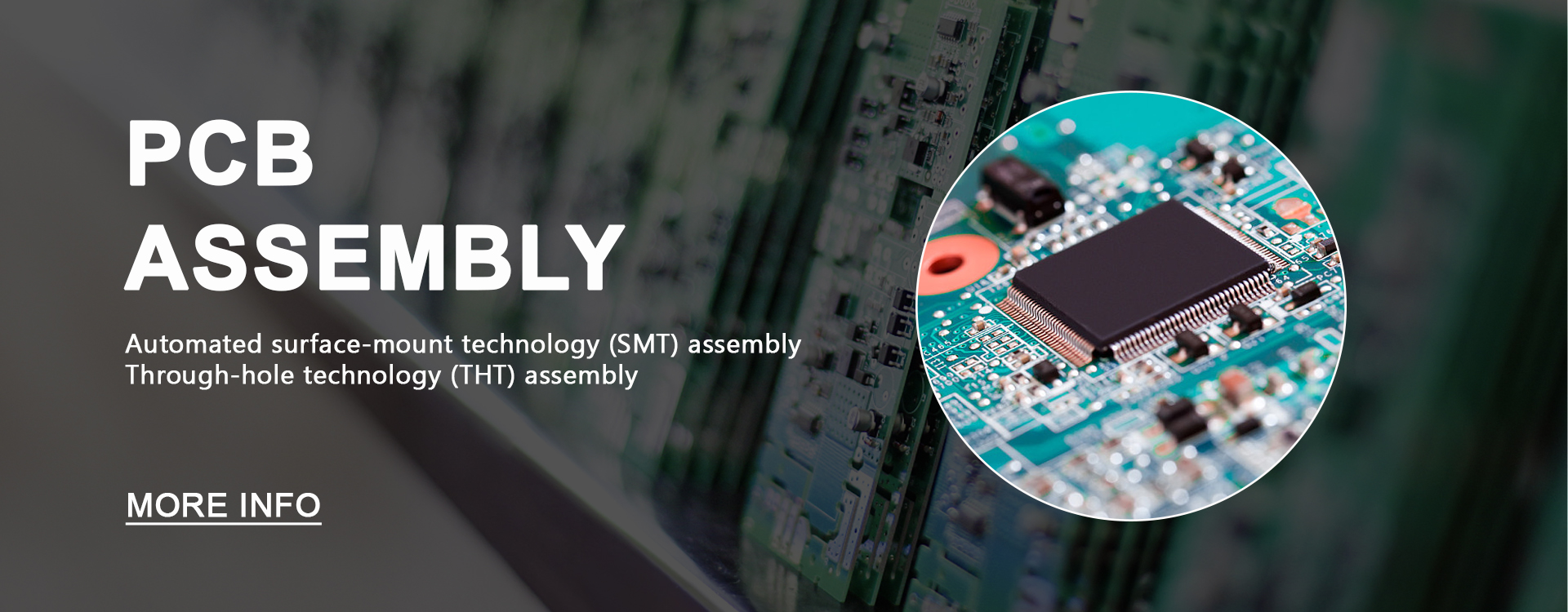
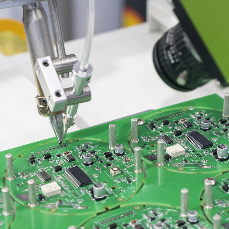
      SMT (Surface Mount Technology) and DIP (Dual - In - Line Package) are two different methods of component mounting on a PCB. SMT involves mounting small - sized components directly onto the surface of the PCB, usually using automated pick - and - place machines and reflow soldering. DIP, on the other hand, uses components with leads that are inserted through holes in the PCB and then soldered, often used for larger or more traditional components.

    • PCB Assembly Rework

      PCB Assembly Rework refers to the process of making corrections or modifications to an already - assembled PCB. This can involve tasks such as replacing defective components, repairing soldering joints, or making design - related changes. Rework is often necessary to salvage boards that have failed initial testing or to upgrade existing assemblies.

    • SMT Stencil

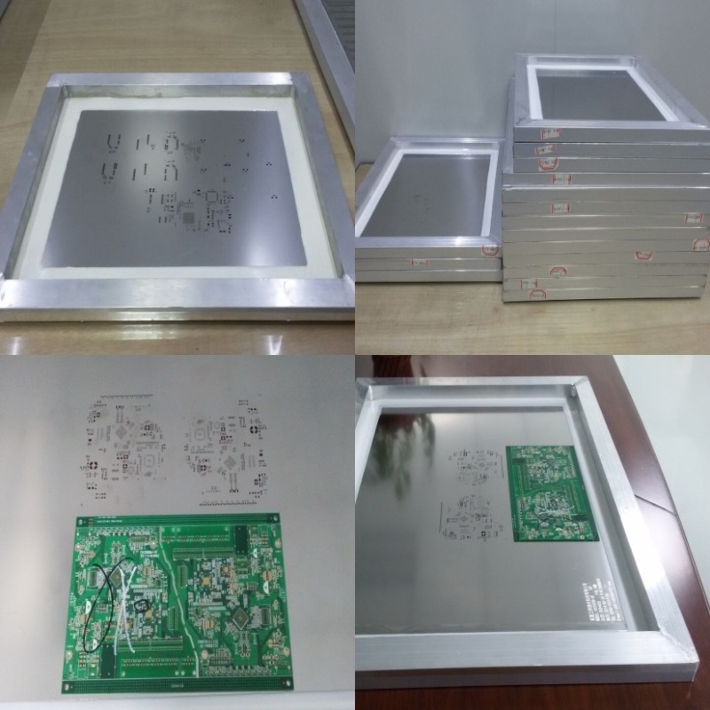
      An SMT stencil is a crucial tool in the SMT process. It is a thin metal or polymer sheet with precisely - cut openings that correspond to the solder pad locations on a PCB. During the solder paste application step, the stencil is placed over the PCB, and solder paste is squeegeed through the openings to deposit the correct amount of solder paste onto the pads, ensuring accurate and consistent component soldering during the SMT process.