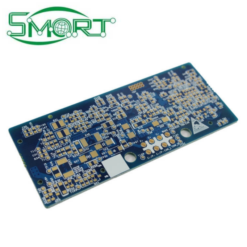
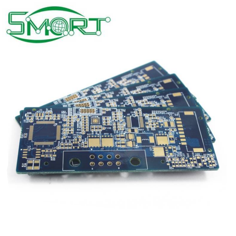
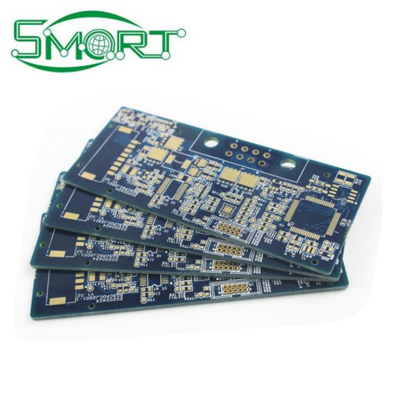
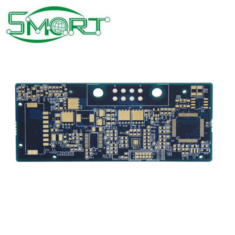
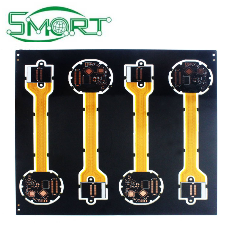
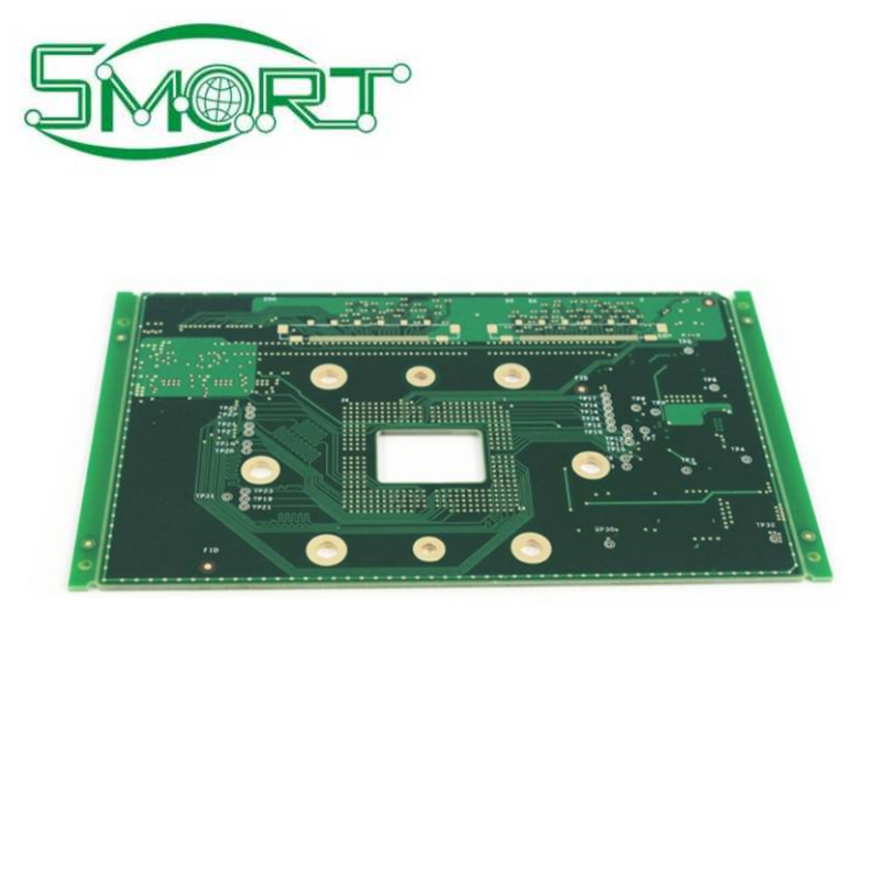
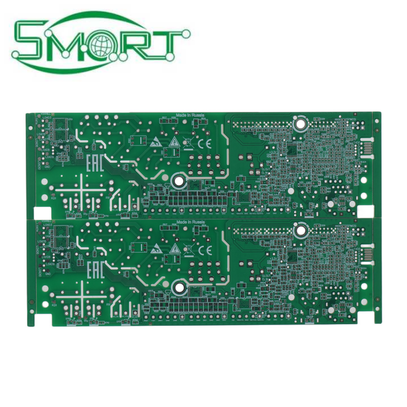
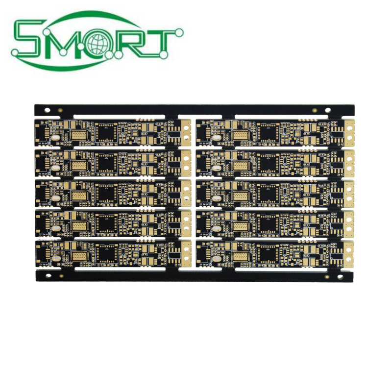
Smart Electronics Blue Solder Mask 8 layer gold-plated impedance ENIG PCB board
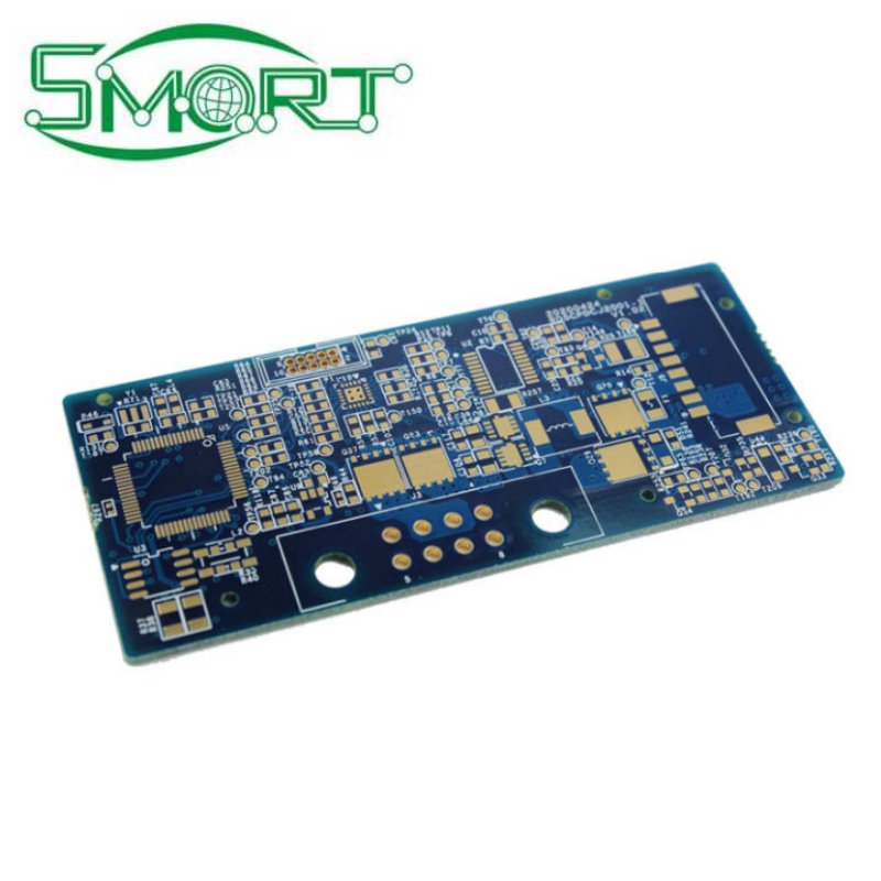
Smart Electronics Blue Solder Mask 8 layer gold-plated impedance ENIG PCB board

The 8-layer gold-plated impedance ENIG (Electroless Nickel Immersion Gold) PCB board is a highly advanced and sophisticated printed circuit board.
This PCB board features eight layers of conductive materials and insulating substrates, which provide enhanced routing capabilities and allow for more complex circuit designs. The gold plating offers several significant advantages. Firstly, it provides excellent electrical conductivity, ensuring reliable signal transmission and low contact resistance. This is crucial for high-frequency and high-speed applications where signal integrity is of utmost importance.
The impedance control feature is another key aspect of this PCB board. By precisely controlling the impedance of the circuit traces, signal reflections and distortions can be minimized, resulting in improved signal quality and reduced electromagnetic interference. This is particularly important in applications such as telecommunications, networking, and high-performance computing.
The ENIG surface finish provides a number of benefits as well. Electroless nickel provides a barrier layer that protects the copper traces from oxidation and corrosion, while the immersion gold layer provides excellent solderability and a noble metal surface that is resistant to tarnishing. This combination of finishes ensures long-term reliability and durability of the PCB board.
The manufacturing process of an 8-layer gold-plated impedance ENIG PCB board is complex and requires advanced technology and expertise. Precise layer alignment, high-resolution imaging, and controlled plating processes are essential to ensure the quality and performance of the board.


