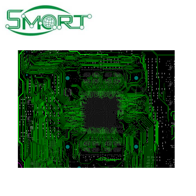
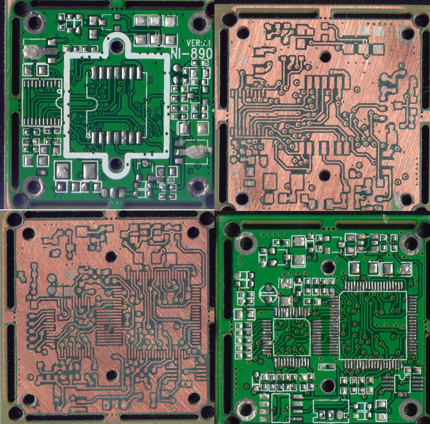
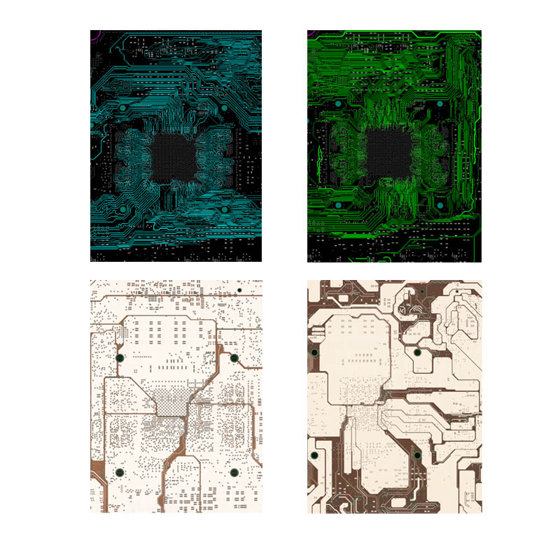
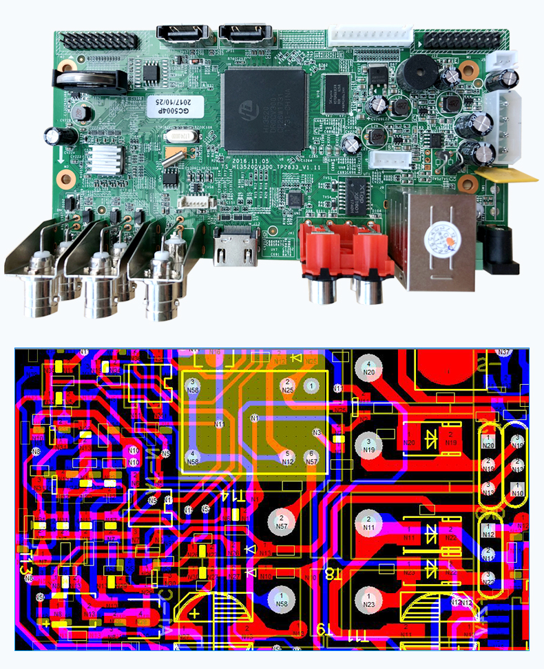
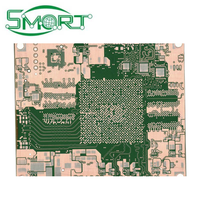
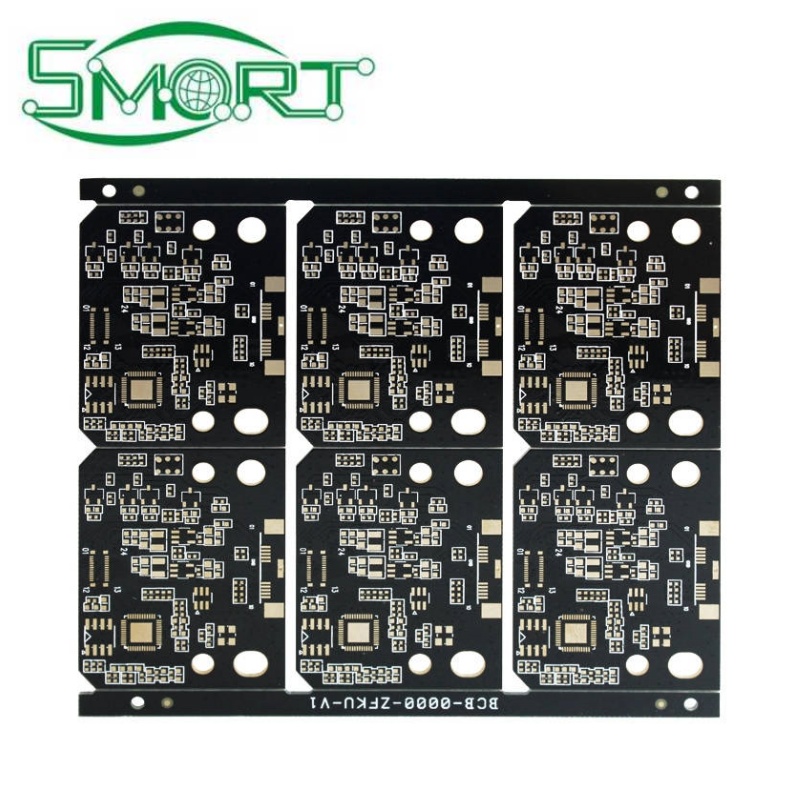
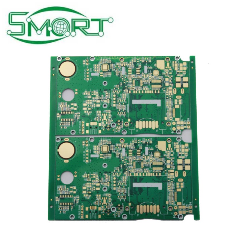
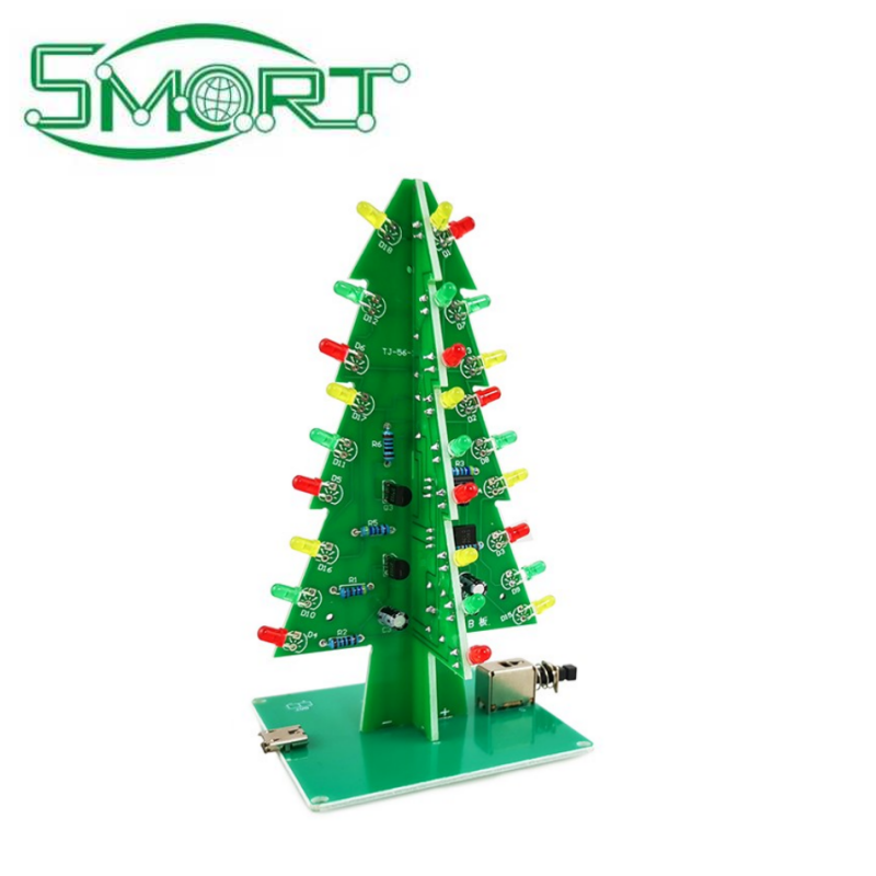
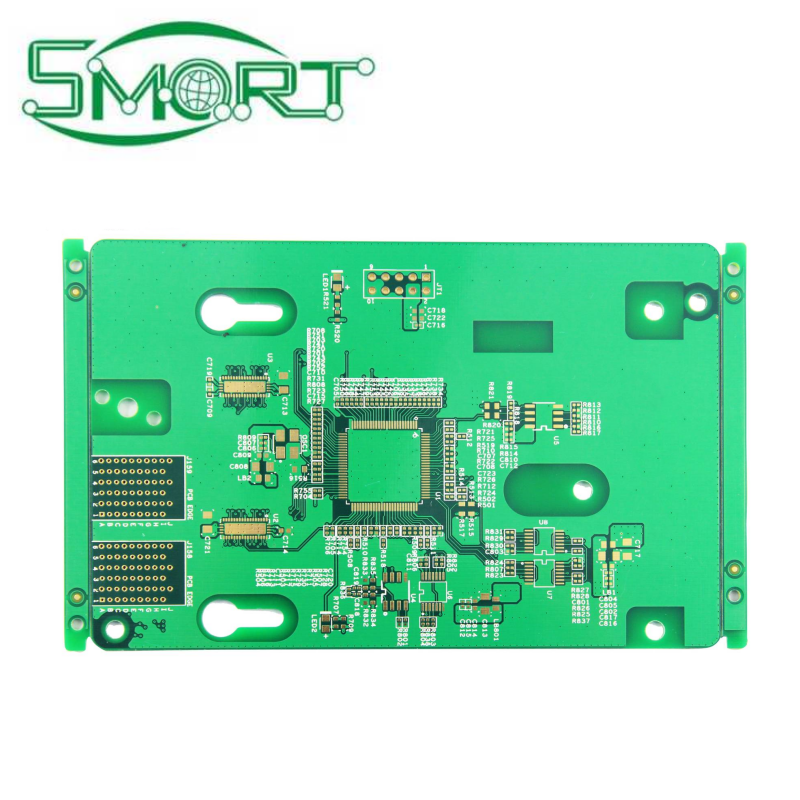
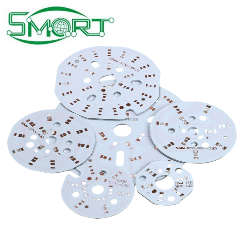
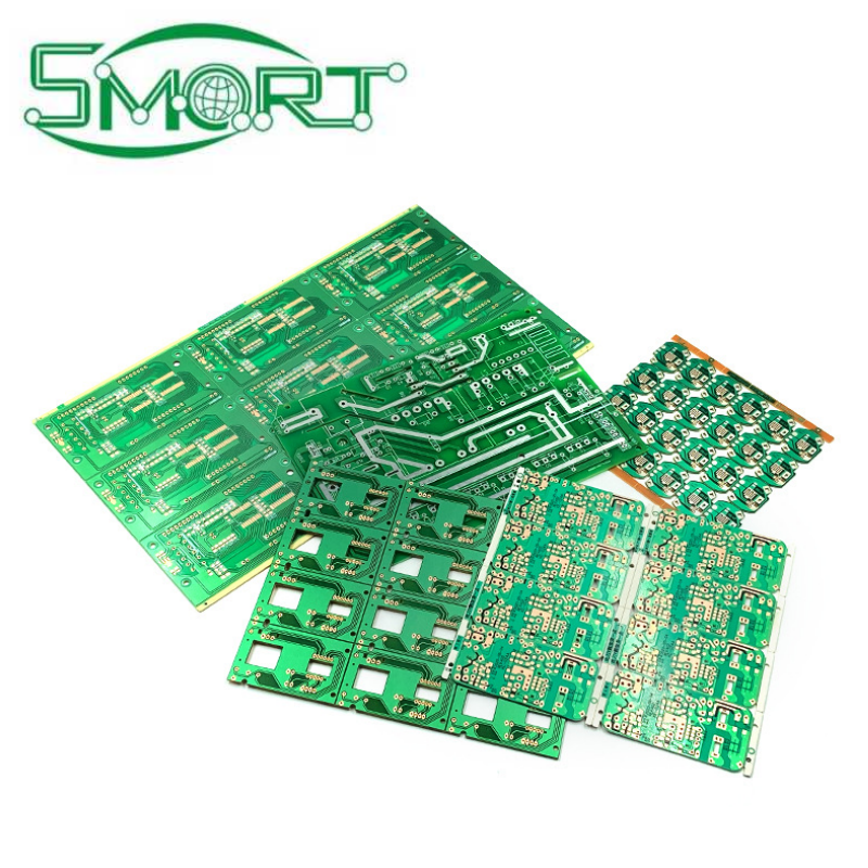
Smart Electronics China Shenzhen PCB, PCBA cloning , PCB manufacture and assembly

Products > PCB > Smart Electronics China Shenzhen PCB, PCBA cloning , PCB manufacture and assembly

Smart Electronics China Shenzhen PCB, PCBA cloning , PCB manufacture and assembly

China Shenzhen PCB, PCBA cloning , PCB manufacture and assembly
shared:


Product Name
Custom Electronic Printed Circuit Board PCB Assembly Services OEM Other Multilayer PCB PCBA Manufacture
Our Service
Electronic Engineering; PCB Manufacturing; Turnkey PCBA; PCB Clone; SMT; Component Sourcing; PCB Assembly; Plugin Assembly; PCBA Clone, PCB Packing Ect.
Main Product Applacation
Household Appliance; Medical Products; Communication Products; Network Device; Gate Way Control; Automotive Products; Industrial
Products; Consumer Electronics; Aviation; Renewable Energy Ect.
Certificate
CE; RoHS; ISO9001;FCC;EPR_Germany_WEEE;EPR_France_WEEE

PCB Capacities and Technical Specification
Order Quantity
1-500,000
Layer
1, 2, 4, 6, up to 24 layer
Material
FR-4, High Tg, Isola, Aluminum, Rogers, etc
PCB type
Rigid, flexible, rigid-flexible
Shape
Rectangular, round, slots, cutouts, complex, irregular
Max PCB dimensions
1200mm*600mm
Thickness
0.2~4.0mm, Flex 0.01~0.25''
Thickness tolerance
± 10%
Copper thickness
0.5-6 oz
Copper thickness tolerance
± 0.25oz
Surface finish
HASL, LF HASL, Imm Gold, Imm Silver, OSP etc
Solder mask
Green, red, white, yellow, blue, black, orange, purple
Silk screen
White, black
Silk screen min line width
0.006'' or 0.15mm
Min drill hole diameter
0.01'', 0.1mm or 10 mil
Min trace/gap
0.075mm or 3mil
PCB cutting
Shear, V-score, tab-routed
PCBA Capacities and Technical Specification
PCBA
PCB+components sourcing+assembly+package
Assembly details
SMT and Thru-hole, ISO SMT and DIP lines
Lead Time
Prototype : 15 work days. Mass order : 20~25 work days
Testing on products
Testing jig/mold , X-ray Inspection, AOI Test, Functional test
Quantity
Min quantity : 1pcs. Prototype, small order, mass order, all OK
Files needed
PCB : Gerber files(CAM, PCB, PCBDOC)
Components : Bill of Materials(BOM list)
Assembly : Pick-N-Place file
PCB Panel Size
Min size : 0.25*0.25 inches(6*6mm)
Max size : 1200*600mm
Components details
Passive Down to 0201 size
BGA and VFBGA
Leadless Chip Carriers/CSP
Double-sided SMT Assembly
Fine Pitch to 0.8mils
BGA Repair and Reball
Part Removal and Replacement
Component package
Cut Tape, Tube, Reels, Loose Parts
PCB+ assembly process
Drilling-----Exposure-----Plating-----Etaching & Stripping-----Punching-----Electrical Testing-----SMT-----Wave Soldering-----Assembling-----ICT-----Function Testing-----Temperature & Humidity Testing


Name
Phone
Email
Corporate name
Address
Leaving Message*
 
Verification code
Submit